A more formal analysis about why the previous compensation scheme worked.
On this first part I will cover the loop around the opamp ignoring for a while the output transistor and parasitic capacitances; they will come later.
Some math after the jump.
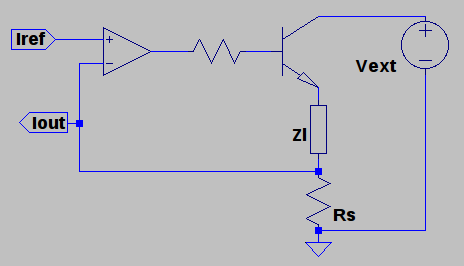
So after a while I went for a more minimalistic approach. This is more or less the original load:

Original circuit of the active load.
The opamp power supply is not shown, Vext and Zl are external to the circuit. Assuming for a while that the opamp is a bit more ideal and its output can swing to at least Vext the circuit can be reorganized as follows without changing the behaviour:
Active load circuit, reorganized.
And finally, we can dispense of the transistor, arriving at the bare minimum:

Active load, simplificated.
If Zl is an inductor we can model it as a ‘pure’ inductor L in series with a resistance Rl. Then, the voltage at Iout will be:

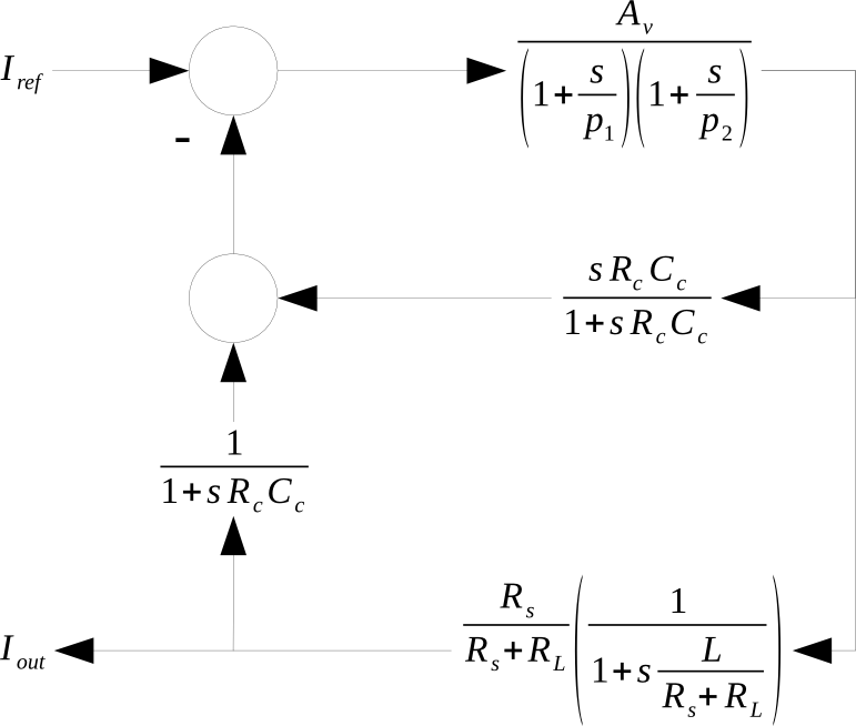
We can build a block diagram of the whole system:

Uncompensated system.
So we have a three pole system (p1 and p2 are the opamp poles). This is bound to oscillate sooner or later unless gain is reduced or the response modified with a compensation network.
The traditional recipe for this cases is to put a small capacitor from the output to the inverting input of the opamp. Given the very low impedance present at V- we isolate it with a moderate resistor, thus the new circuit is:

Compensated active load.
To obtain the voltage at Vfb we use the superposition theorem. Neglecting the loading effect that Rcc and Cc can present at the Vout and Iout nodes we consider the two cases:

Models of the compensation network for Iout and Vout to Vfb
For Vout it acts as a high pass filter and as a low pass for Iout. In the s domain that is:

And in a block form:
Compensated system.
The denominator of the transfer function is then:
![1 + \frac{A_v}{(1 + s / p_1) (1+ s / p_2)} \frac{1}{1 + s R_c C} \left [ s R_c C + \frac{R_s}{R_s + R_L}\frac{1}{1 + s \frac{L}{R_s + R_L}} \right]](https://s0.wp.com/latex.php?latex=1+%2B+%5Cfrac%7BA_v%7D%7B%281+%2B+s+%2F+p_1%29+%281%2B+s+%2F+p_2%29%7D+%5Cfrac%7B1%7D%7B1+%2B+s+R_c+C%7D+%5Cleft+%5B+s+R_c+C+%2B+%5Cfrac%7BR_s%7D%7BR_s+%2B+R_L%7D%5Cfrac%7B1%7D%7B1+%2B+s+%5Cfrac%7BL%7D%7BR_s+%2B+R_L%7D%7D+%5Cright%5D&bg=ffffff&fg=000&s=2&c=20201002)
With a bit of algebra the term on square brackets can be simplified as follows:

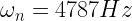
So, now we have a system with four poles and two zeros. The natural frequency and damping factor are:


Most of the time the damping factor will be quite low. One of my problematic loads was a 4mH choke with about an ohm of series resistance. Plugging that values and using Rc = 10K and Cc = 120pF (just had those at hand) I get:

Which results in a pair of complex zeros at 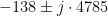
The net effect of this pair of zeros is to move the root locus towards the left side of the complex plane, stabilizing the system. Using Octave we can easily plot it:

Root locus of compensated system.
It is noteworthy the high amount of gain that is needed for the poles to move close to the zeroes.